Download this article in PDF format.
5G is poised to revolutionize connectivity, providing a programmable, intelligent connection between users and cloud services as well as a seamless, ubiquitous and personalized experience across different environments and devices. With one network for all use cases required by the Big Data explosion, from home to enterprise environments, 5G promises to connect tens of billions of devices that are always online, each with their own slice of the network, dynamically established to provide a dedicated profile of priority, security, speed, and latency.
To realize the convergence of cloud and telecommunications services, the 5G rollout requires significant infrastructure changes to the existing network, both for New Radio (NR) access and backhaul as well as in the core, to bridge wireless and wired networking. Changes include more, smarter radio-frequency (RF) devices to increase network coverage and capacity; more intelligence on demand in the network; and localization of functions in the cloud or at the edge, according to the required level of network service.
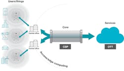
The new network scenario (Fig. 1) includes significant changes in the NR access network portion to enable higher capacity and coverage, while also requiring that the core networks follow the bandwidth requirements in the switching and optical elements. There is also the introduction of new systems, like mobile edge computing.
1. 5G transforms the network scenario, adding new end equipment.
Dealing with Density
The entire segment industry is contributing new hardware that will enable 5G. The drive to achieve 5G network speeds up to 10 Gb/s in bandwidth—achieved by increasing RF signals to centimeter and millimeter wave in the second phase of 5G deployment, as well as multiple-input mulitple-output (MIMO) beamforming and new, multibandwidth active antenna systems (AASs) to increase spectrum efficiency—creates an extremely challenging hardware environment from a space-density perspective. Similar challenges already exist with macro radio base stations operating at higher frequencies and with multiple power-amplifier (PA) structures and MIMO small cells.
On the signal-chain side, density is enabled by the adoption of high-speed, multiband, multichannel transceivers, up to four receivers/transmitters (Rx/Tx) and 1-GHz bandwidth, that employ RF and zero-intermediate-frequency sampling techniques. New, integrated signal-chain components have increased power needs, an obvious requirement for the increasing numbers of PAs. Power per PA decreases while overall power per system increases, requiring a change in architecture to supply that power. Meanwhile, it’s necessary to satisfy the low-noise requirements of each specific radio implementation.
The Converter Factor
An extremely constrained space requires an increased converter switching frequency in order to still fit without efficiency penalties, despite the difficult thermal environment: fully encapsulated, no forced ventilation, and an extremely high (albeit controlled) printed circuit board (PCB) temperature as high as 100°C.
New controller techniques enable converters to meet the requirements of this application environment. Advanced current mode with adaptive gate drive facilitates smooth controller transitions even at high switching frequencies, offering lower noise behavior and improving reliability while reducing the minimum on-time. Packaging is also critical to enable increased switching frequencies and the dissipation of associated losses. Conduction losses, reduced by exceptionally efficient power stages, compensate for that incremental factor for total power consumption. Designers must trade off the maximum switching frequency with the maximum junction temperature over operation and reliability considerations.
Dissipation comes into play, especially when a heat sink is available closer to the RF or system-on-chip (SoC) section. Converters can leverage this heat sink to extract heat from the top. It’s possible to reduce the junction temperature if the package offers resistance to the top, comparable even if higher to the bottom, where most of the heat is already directed to be transferred to the PCB. There, it’s thermally shunted to the mechanical encapsulation and controlled thermally, modulating the value of input power.
With the 4X increase in transceiver density when implementing the entire analog front-end (AFE) function—with four digital-to-analog converters/four analog-to-digital converters, an oscillator, filtering, and mixing on the same chip—power needs to follow a similar scale of integration. However, considering the multiplication factor introduced by MIMO AASs, when moving from a 4x Tx/Rx configuration to a 64x or 128x Tx/Rx configuration, the scale factor cannot be linear.
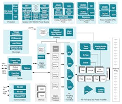
It might be possible to integrate one system power solution for more than four AFEs. The converters must supply clusters of multichannel transceivers, respecting the signal-chain integrity at those sensitive points of the RF path. Texas Instruments’ AAS block diagram (Fig. 2) shows the fundamental elements that constitute this NR element (Fig. 3).
2. TI’s AAS block diagram shows the fundamental subsystems of the application.
3. AASs enable MIMO and multiband operation, providing electronic 3D beam control.
Devising an Efficient Power Subsystem
Looking at power subsystems, due to increased power/current—in some cases over 1 kW—a 12-V intermediate bus voltage is common. Other architectural elements now becoming mainstream include multichannel converters and low-dropout (LDO) regulators as well as low-noise converters, which could help improve total system efficiency. These reduce the need for low-noise LDOs with a high power-supply rejection ratio, which are sometimes used across the most critical rails, from phase-locked loop to serializer-deserializer. The point-of-load switching frequency must be higher than 1 MHz to enable a size reduction of passive components.
Combining rails where possible avoids the risk of AFE crosstalking and interference, while still respecting the tight voltage tolerances of the rails and sequencing specifications among different rails. LDOs can provide the simplest sequencing (PG/EN), and that can sometimes be a reason to add some to the bill of materials (BOM). If required by the integrated transceiver, negative rails require special effort in the converter. A large ripple in the output makes a simple buck-boost topology an unwise choice.
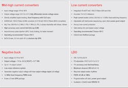
Placing several integrated transceiver rails on the board within a reasonable distance (drop) and achievable noise immunity simplifies the schematic by reducing the number of converters, mainly LDOs, that are used to separate and supply different AFEs locally. Figure 4 provides a potential BOM of converters and LDOs that can fit the application, with a detailed list of critical parameters.
4. The main characteristics of power devices supplying a multi-AFE solution are shown.
A Power Solution
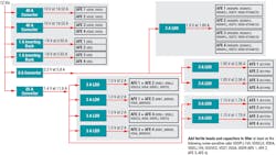
Figure 5 is a block diagram of a power solution with four integrated transceivers, implementing many of the considerations described above. Ferrite beads aren’t shown in the figure, but they’re necessary (with associated capacitors) to decouple crosstalk of clustered inputs of the transceiver, inside the single one, and with respect to the others clustered with the same power solution—at least on the noise-sensitive rails. Some next-generation transceivers have lower power-consumption levels that can potentially enable clustering of as many as eight integrated transceivers if the mechanical constraints of the board layout allow.
5. This simplified block diagram illustrates a power solution for four AFEs.
To evaluate the quality of the power-supply solution, consider these specifications for Rx and Tx performance:
- Rx: signal-to-noise ratio, spurious-free dynamic range, and intermodulation distortion from third order.
- Tx: phase noise and third-order intercept.
You must measure these parameters on the AFE with your proposed power solution to investigate any impact in performance, resolving any issues by filtering, using ferrite beads or changing the power BOM if the issue is more significant.
Timing
Much like with RF transceivers, with power challenges come new clocking requirements. The new Ethernet-based common public interface (eCPRI) creates a need for timing and frequency synchronization in multipoint connections between the baseband unit (BBU) and remote radio unit (RRU), and challenging delay requirements in the clock tree in a beamforming implementation. Companion system power solutions must minimize BOM and cost as well as increase density while maximizing features with low noise performance and efficiency at higher switching frequencies.
It’s possible to combine the same solution for RF transceivers and clocking, following the criteria described earlier, to generate an effective power solution for a specific 5G radio or BBU. The Power Management Bus (PMBus) and Serial Voltage Identification interfaces have a fundamental importance in BBUs, even more than in RRUs. They must be available in controllers and converters for multiphase and single-rail solutions in order to power the latest processing SoCs, achieve fast transient performance, and accurately monitor parameters for performance optimization and system reliability.
The cloudization of the BBU, where a centralized BBU connects to many RRUs, requires more functionality inside the RRUs, causing power to increase. The higher power requires adaptive output voltage scaling through PMBus.
Another hot area for power integration is the PA bias portion, which requires 65-V operating converters with a variable current limit as high as 5 to 6 A. Thermal considerations limit the switching frequency. As a compromise to size reductions, the thermal performance of the package is key to enabling a reliable junction temperature, even in the extreme 5G radio ambient. When power exceeds the limit for single-package solutions, solutions based on controller and external field-effect transistors are also viable, especially when combining several PA supplies into a single-power solution.
Conclusion
Intelligent connectivity provided by the 5G network will affect several industries and enable new services. Thanks to 5G innovation, these are just some of the great technological advances we will soon enjoy:
- Continuous health monitoring with fully secure and reliable real-time connections.
- Reliable and low-latency remote control of applications, realized with proprioception and tactile internet.
- Efficiency improvements in production lines, with sensor data collection and interactive robots.
- Holographic projection of remote trainings and events.
Smart power requirements for 5G technologies require dedicated components to achieve the best density and efficiency, and survive the extreme thermal conditions of the environment. It’s important to resolve technical challenges with next-generation power components, enabling efficiency at high frequencies for maximum density, through innovative control topologies and packaging techniques.
Pietro Scalia is Sector General Manager, Communications Equipment and Enterprise Systems, at Texas Instruments.
References
Scalia, Pietro, Mark Ng, and Ryan Manack. “Optimum Powering of Signal Chain in 5G AAS m-MIMO Architectures,” APEC 2018 Conference.
Scalia, Pietro. “Preparing for a 5G world: An overview of the enabling technologies and hardware requirements,” TI.com white paper.


