How to Solve Complex Adhesion Problems With Plasma Pen Technology
Plasma is a state of matter, like a solid, liquid, or gas. When sufficient energy is applied to a gas, it becomes ionized, transitioning into the plasma state. With precise application and control, plasma can alter the surface properties of a metal or plastic part without compromising the underlying material.
Although plasma has a wide range of applications, it's frequently used to improve the adhesion of chemical glues, printing inks, and coatings. This is often the best—and only—solution for manufacturers facing persistent challenges such as high failure rates caused by delamination, inadequate bonding, poor surface printing, or issues with coating adhesion.
"Plasma contains ions, electrons, neutral particles, and reactive species that can be utilized for precision cleaning, decontamination, increasing surface "wettability," and other surface modifications. These techniques can boost the bond strength by up to 50 times in certain cases," says Ryan Blaik, Sales Manager of Corona-based PVA TePla.
While there are multiple methods for applying plasma to a product's surface, one of the most popular and accessible are plasma "pens". These tools ionize gas, such as air or noble gases, under normal [atmospheric] pressure conditions using electrical discharges.
"The plasma produced from the tip of the pen can be applied to very specific areas or the entire part," Blaik explained, adding that often plasma pens are incorporated into automated inline manufacturing processes or controlled by robots.
According to Blaik, plasma pens serve as an affordable introduction to plasma technology. Unlike traditional vacuum-based plasma chambers where parts are processed in high-volume batches, the plasma pen can be installed inline, requires less energy, and incurs lower operational costs. Other advantages include reduced upfront investment, simplified exhaust management, and suitability for smaller-scale production requirements.
"For manufacturers that only need to spot treat a part or operate high-speed production lines, a solution as simple as a pen may make more sense," says Blaik. "Plus, if you are comparing the cost, a pen is going to be more affordable than a larger batch processing system."
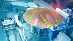
Today, plasma pens have already been adopted in the automotive, aerospace, electronics, medical devices, and packaging industries. Current uses include improving adhesion for Anisotropic Conductive Film (ACF) in flat-panel display assembly, manufacturing silicon photovoltaic cells, assembling thin-film photovoltaic modules, and bonding polymers with adhesives. Additional applications include enhancing the performance of inks, dyes, paints, potting materials, over-molding, under-fill compounds, and various biomaterials.
How Plasma Pens Solve Complex Adhesion Challenges
For most applications, plasma treatments are used to increase the surface-free energy of the material. Surface energy is defined as the sum of all intermolecular forces that are on the surface of a material, the degree of attraction or repulsion force of a material surface exerts on another material.
When a substrate has high surface energy, adhesives, and other liquids often spread more easily across the surface. There are several mechanisms for increasing surface energy with plasma, including precision cleaning, chemically or physically modifying the surface, increasing surface area by roughening, and applying primer coatings.
"Most materials are initially hydrophobic [they repel water]. To make them bondable, their surface is typically modified to become hydrophilic [attract water]," explains Blaik. "The plasma pen excels at making raw materials hydrophilic, enhancing their ability to bond effectively with chemical adhesives."
The plasma pen is particularly effective for preparing materials in overmolding processes, including polypropylene applications, dip coatings, or any method that involves encasing or encapsulating components.
"The key aspect is enhancing the surface's wettability," says Blaik. "This allows the overmold to spread more effectively across the surface and minimizes the formation of bubbles or air gaps caused by low-energy surfaces. The result is a stronger and more reliable bond."
A common application of silicone overmolding is to safeguard electronic boards against exposure to outdoor weather conditions. Without proper adhesion, silicone can begin to delaminate, not only at the edges of the PCB board but also in the form of small air pockets on, or around, components. This can lead to moisture ingress and subsequent corrosion or electrical shorts.
Another challenge is the topography of a PCB, which means silicone must bond to many types of materials, including polymers, metals, alloys, ceramics, and the FR-4 board itself, all of which have unique surface energies and chemistries.
PVA TePla developed a specific process starting with a precision cleaning/surface activation treatment followed by the deposition of an inert chemical primer that serves as a tie layer for the overmolding and provides a uniform surface energy for the silicone to bond.
Plasma generated from atmospheric air exhibits strong oxidative properties, making it highly effective for surface cleaning and activation. Layers of absorbed molecules, such as oil and water on metallic surfaces, can be easily removed to improve adhesion.
Surface cleaning is also used in some cases to improve electrical contacts by cleaning oils and any organic debris from electrical contacts to ensure a better connection. One example is gold pads, the gold-plated contact points on a printed circuit board (PCB) that connect to other electronic components to transmit power, signals, and data. Other cleaning applications include wire and die bond pads, fiber optic cables, weld lines, and optics.
Atmospheric plasma can also be used to oxidize the surface of plastics to promote the adhesion of materials like inks, adhesives, or coatings.
Choosing a Plasma Pen
Atmospheric plasma pens can generate two forms of plasma: Blown plasma and corona discharge.
Blown plasma is created at atmospheric pressure and expelled through a nozzle using a carrier gas, typically air, nitrogen, or other inert gases. The gas flow produces a plasma plume capable of treating larger surface areas.
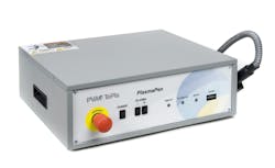
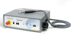
PVA TePla's PlasmaPen, for example, can deliver a directed beam 3 to 10 mm (0.1 to 0.4 in) wide, with a plume length of up to 14 mm (0.5 in).
Process gasses flow through the PlasmaPen assembly and are activated and ejected through the nozzle. The patented design keeps high voltages and current safely inside the pen body, away from the plasma jet and substrate surfaces. The absence of electrical voltage in the plume allows heat-sensitive or electrically delicate materials like polymers, textiles, or electronics to be treated.
"Since the plume is electrically neutral, there is no risk of electrical arcing or damage to sensitive components," says Blaik.
Corona discharge plasma is the other alternative and is among the most commonly available pen types on the market. In this approach, a high-voltage electrical field is created to ionize a localized region of gas, creating plasma.
The strong electric field enables effective treatment of tough surfaces, and the discharge can be highly targeted, making it ideal for precision surface treatments in small or difficult-to-reach areas.
However, the downside is the electrical discharge, which eliminates its use in heat-sensitive materials and sensitive materials.
In some systems, corona discharge can be "blown" by introducing a gas flow. This method is effective for covering larger areas or distributing energy more evenly. However, this approach has limitations, as the plume's length is relatively short, and the process still relies on the presence of an electrical discharge.
Plasma Pen Customization Options
Although plasma pens follow a standard design, significant variations exist between different models. Manufacturers like PVA TePla provide various options and customizations to meet specific needs, including adjustments to the aspect ratio of the plasma plume, intensity, and dwell times.
According to Blaik, "When atmospheric plasma is delivered by a pen, a significant amount of heat is produced and it can cause scoring and marking of plastic or composite surfaces."
PVA TePla addressed the issue by designing a pen head with extra cooling channels to keep the tip cooler. The company also offers different pen tips to control the aspect ratio of the plasma plume.
"With a plasma pen you need to be able to fine-tune the distance of the plume from the surface to control the intensity, while also considering the dwell time," explains Blaik.
Even the angle of the approach can be a factor.
"If you are blowing plasma straight down at a 90-degree angle, you could potentially blow the contaminant that you are cleaning off back onto the surface,” said Blaik.
For this reason, PVA TePla recommends tilting the pen at a 30 to 60-degree angle so the plasma can bounce off the surface and leave a cleaner surface that is better for bonding.
Plasma Pen Integration Options
Plasma pens can be easily integrated into existing inline processes with different degrees of automation. This flexibility is particularly beneficial, as plasma treatments are often introduced after initial processes have been validated, typically in response to high failure rates.
"Our PlasmaPens allow customized programming and integration into any manufacturing line concept, and we can partner with any robot manufacturer," says Blaik.
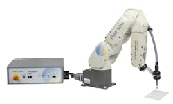
PVA TePla also offers automated packages that include multiaccess robots or even a Cartesian robot. The company's RoboPen provides multiaxis or X, Y, and Z robotic operations and can be customized to meet a broad variety of manufacturing applications.
When more than a spot application is required, the pen can be programmed to raster back and forth over the surface to treat a complete part. Other alternatives include moving the pen by multiaxis robot around a stationary part or keeping the pen stationary and moving/rotating the part.
Plasma technology has changed how manufacturers address persistent adhesion challenges, and plasma pens provide an accessible and cost-effective gateway for industries to harness its benefits.
By leveraging plasma pen technology into inline processes, manufacturers can achieve stronger, more reliable bonds, improved wettability, and enhanced performance across various materials. With their ability to precisely treat surfaces, improve adhesion, and enhance surface energy, plasma pens have become an indispensable tool in a wide range of industries, from automotive to electronics and medical devices.
For more information, contact PVA TePla America at (951) 371-2500 or (800) 527-5667, email [email protected], or visit pvateplaamerica.com.
About the Author
Jeff Elliott
Jeff Elliott is a Torrance, CA-based technical writer.