Overcoming Hybrid Bonding Challenges: The Role of Scanning Acoustic Microscopy in Semiconductor Manufacturing
Today, hybrid bonding is transforming the semiconductor industry by facilitating the production of increasingly intricate, efficient, and powerful electronic devices. This advancement is beneficial for artificial intelligence (AI), high-performance computing, and graphics processing units (GPUs).
The reason hybrid bonding is quickly gaining recognition is due to the enhanced reliability and mechanical strength of its interconnects, as well as the space savings compared to traditional bump-based interconnections. This bonding technique vertically links die-to-wafer (D2W) or wafer-to-wafer (W2W) via closely spaced copper pads, bonding the dielectric and metal bond pads simultaneously in a single bonding step.

Hybrid bonding offers several significant benefits, including allowing a higher density of interconnections with shorter pitches and less distance between the layers. These factors improve signal integrity, reduce latency, lower power consumption, and increase data throughput. Furthermore, hybrid bonding facilitates heterogeneous integration, enabling semiconductor companies to merge multiple chiplets with diverse functions, technology nodes, and sizes into a unified package.
However, to successfully transition to high-volume manufacturing with high yields requires advanced metrology tools that can quickly identify defects like cracks and voids within the bonded layers.
“The concept behind three-dimensional advanced packaging is to stack multiple dies or wafers vertically to achieve better performance with lower power requirements, smaller size, and lower cost,” says Hari Polu, President of PVA TePla OKOS, a Virginia-based manufacturer of SAM and industrial ultrasonic non-destructive (NDT) systems. The company serves the semiconductor, electronics, aerospace, metal/alloy/composite manufacturing, and end-user markets.
“However, as three-dimensional packages become increasingly complex, so do the challenges in identifying defects within vertically stacked, multiple layers. Now, the focus is shifting to methods of non-destructive testing like Scanning Acoustic Microscopy,” adds Polu.
According to Polu, Scanning Acoustic Microscopy (SAM) is a non-invasive and non-destructive ultrasonic testing method that is quickly becoming the preferred technique for testing and failure analysis involving stacked dies or wafers.
SAM uses ultrasound waves to non-destructively examine internal structures, interfaces, and surfaces of opaque substrates. The resulting acoustic signatures can be constructed into 3-dimensional images that are analyzed to detect and characterize device flaws such as cracks, delamination, inclusions, and voids in bonding interfaces, as well as to evaluate soldering and other interface connections.
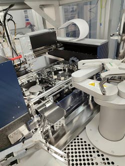
“With conventional SAM techniques, wafers were held horizontally in a chuck and processed in a water medium, and this occasionally could lead to water ingress, trapping water, which could cause significant issues in the next step of assembly. By re-designing the chuck in a vertical orientation, we can use gravity to eliminate any concern over water ingress, along with other water management technologies."
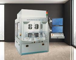
SAM is already the industry standard for 100% inspection of semiconductor components to identify defects such as voids, cracks, and delamination within microelectronic devices.
Now the technology has been adapted to facilitate 100% inspection of hybrid bonded packages.
“Innovations in the design of wafer chucks, array transducers, and AI-based analysis of inspection data are converging to provide a more robust SAM solution for fabs involved in hybrid bonding,” says Polu.
Solving the Hybrid Bonding Inspection Challenge
With hybrid bonding, various steps must be reliably performed to ensure quality, with any failures resulting in unacceptable defects. The stakes are higher than ever considering that even one bad wafer, die, or interconnection could cause the entire package to be discarded down the line. Sub-10-micron defect detection is the new normal.
The process begins by manufacturing the wafers or dies in a semiconductor fab before the chips are bonded together. Typically, the key process steps include the preparation and creation of the pre-bonding layers, the bonding process itself, the post-bond anneal, and the associated inspection and metrology at each of the steps.
“With conventional SAM techniques, wafers were held horizontally in a chuck and processed in a water medium, and this occasionally could lead to water ingress, trapping water, which could cause significant issues in the next step of assembly. By re-designing the chuck in a vertical orientation, we can use gravity to eliminate any concern over water ingress, along with other water management technologies,” says Polu.
Scanning acoustic microscopy works by directing focused sound from a transducer at a small point on a target object. The sound hitting the object is either scattered, absorbed, reflected, or transmitted. By detecting the direction of scattered pulses as well as the “time of flight,” the presence of a boundary or object can be determined as well as its distance.
To produce an image, samples are scanned point by point and line by line. Scanning modes range from single-layer views to tray scans and cross-sections. Multi-layer scans can include up to 50 independent layers. Depth-specific information can be extracted and applied to create two and three-dimensional images. The images are then analyzed to detect and characterize flaws such as cracks, delamination, and voids.
According to Polu, advancements in AI-based analysis of the data collected from SAM inspection of wafer-to-wafer hybrid bonding will further automate quality assurance and increase fab production.
“When fabs take advantage of the higher level of failure detection and analysis, the production yield and overall reliability of high-performance chips improve significantly,” says Polu. “Every fab will eventually move towards this level of failure analysis because of the level of detection and precision required for hybrid bonding.”
Hybrid bonding represents a significant advancement in chip packaging technology, offering numerous benefits that enhance the performance, efficiency, and scalability of semiconductor devices.
Scanning Acoustic Microscopy stands ready to deliver 100% non-destructive inspection of vertically stacked and bonded die-to-wafer (D2W) or wafer-to-wafer (W2W) packages at extremely high speeds to help facilitate the adoption of this technology.
For more information, contact PVA TePla OKOS at [email protected] or visit www.okos.com. PVA TePla OKOS is a wholly owned subsidiary of PVA TePla AG, Germany
About the Author

Del Williams
Del Williams is a technical writer based in Torrance, California. He writes about health, business, technology, and educational issues and has an M.A. in English from C.S.U. Dominguez Hills.