Manufacturers Are Turning to SAM to Increase Electromechanical Sensor Reliability
Electromechanical sensors, such as pressure, flow, and vacuum switches, composed of electrical and mechanical parts, interact and transmit information or commands to other components of a larger, more complex system. To keep the entire system functioning safely, sensor producers need to manufacture these devices to precisely deliver accurate measurements.
Traditionally, however, if there was an issue with a sensor it was often found when the product failed the field. Now, sophisticated testing like Scanning Acoustic Microscopy (SAM) is being used to assess the physical sensing elements to determine whether the components are sound before they are assembled into sensors that will be used in critical applications.
SAM is a non-invasive and non-destructive ultrasonic testing method. The testing is the industry standard for 100% inspection of semiconductor components to identify defects such as voids, cracks, and the delamination of different layers within microelectronic devices. Now, the same rigor of failure analysis and quality testing is being applied to specialty metals and materials to detect subsurface flaws, dis-bonds, cracks, and other irregularities.
“Previously, sensor manufacturers had no way to test the functionality of a sensor until it was in the field. If it gave incorrect results on a known good test, they called it a failure. They had no metrology to test the sensors elements during the manufacturing process,” says Hari Polu, President of OKOS, a Virginia-based manufacturer of SAM and industrial ultrasonic non-destructive (NDT) systems. OKOS is a wholly owned subsidiary of PVA TePla AG, Germany and offers both manual and automated inspection systems for flat panels, thin plates, circular discs, sputtering targets, and special alloys.
Oil Field Sensors
As an example, SAM can be used to ensure sensor quality in oil drilling equipment. These sensors are sensitive to vibrations or generate vibrations at a specific frequency. These sensors provide metrology attributes of fluid properties in real time.
Electromechanical advanced sensors are used in critical areas such as oil field exploration and production processing to take pressure data and fluid samples from the bottom of high-pressure and high-temperature wells. The sensors establish the hold-up of fluids using the density and electrical properties of oil, gas, and water. The characteristics of the vibration can help to determine the density of the wellbore fluid mixture.
“If a manufacturer is building defective sensors and anything fails anywhere in the process upstream, that’s extremely costly for an oil field application. If they find defective sensors in the field downstream, that's also very expensive,” says Polu.
Before shipping, oil drilling equipment manufacturers can test tuning fork sensors’ piezoelectric crystals with SAM to determine if flaws exist. Since piezoelectric ceramics are fragile, sensitive components may present internal cracks undetectable to a visual inspection. Ceramics presenting cracks, even if internal and invisible, must be discarded to avoid the premature fault of ultrasonic transducers and converters in which they are mounted, and the resulting losses from repairs and technical assistance.
Scanning acoustic microscopy works by directing focused sound from a transducer at a small point on a target object. The sound hitting the object is either scattered, absorbed, reflected or transmitted. By detecting the direction of scattered pulses as well as the “time of flight,” the presence of a boundary or object can be determined as well as its distance.
To produce an image, samples are scanned point by point and line by line. Scanning modes range from single-layer views to tray scans and cross-sections. Multi-layer scans can include up to 50 independent layers. Depth-specific information can be extracted and applied to create two- and three-dimensional images without the need for time-consuming tomographic scan procedures and more costly X-rays. The images are then analyzed to detect and characterize flaws such as cracks, inclusions, and voids.
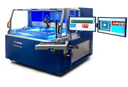
When high throughput is required for 100% inspection, ultra-fast single or dual gantry scanning systems are used along with 128 sensors for phased array scanning. Multiple transducers can also be used to simultaneously scan for higher throughput.
“We’re able to take the SAM technology, which is good at identifying defects in metals, and apply it to detecting the critical parts in sensors so manufacturers don’t release defective products into the field,” says Polu.
Ensuring Lithium Niobate Wafer Quality
Lithium niobate (LiNbO3) is one of the most versatile and well-developed active optical materials that is widely used in electro-optics, acousto-optics, nonlinear optics, waveguides, and fiber optic gyroscopes (FOGs).
One potential application is for oil field sensors. Traditionally, in this application, when cutting, separating, and assembling lithium niobate wafers into sensor housing, only a small percentage prove to be good in the field. The challenge is determining which wafers are defective before incorporation into products.
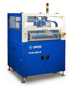
For this type of application, the SAM VUE400 from OKOS is ideal to detect bad wafers prior to use in an electromechanical device. The medium-sized SAM system designed for lab use or manufacturing floors is traditionally used to detect voids, disbands, cracks, delamination, and internal defects in semiconductor package failure analysis. With an ultrasonic digitizer and digital pulse receiver, the system can repeatably scan with an accuracy of +/-0.5 microns.
The SAM equipment can inspect various items with unique product geometry or sizes, from crystal ingots, wafers, and electronics packages to miniature physical packaging, metal bars/rods/billets, turbine blades, etc. However, as important as the physical and mechanical aspects of conducting a scan, the software is the key to analyzing the information to produce detailed scans.
For this reason, “OKOS decided early on to deliver a software-driven, ecosystem-based solution,” says Polu. The company's ODIS Acoustic Microscopy software supports a wide range of transducer frequencies from 2.25 to 230 MHz.
Multi-axis scan options enable A, B, and C scans, contour following, offline analysis, and virtual rescanning for metals, alloys, and composites. This results in highly accurate internal and external inspection for defects and thickness measurement via the inspection software.
Today, manufacturers have the potential to save significant amounts of money per year in oil field sensors or similar applications by detecting and eliminating defective lithium niobate wafers before use in high-value, electromechanical sensors. These savings stem from screening at the wafer level, which prevents packaging and shipping bad products. The total does not even account for substantially improved wafer yields.
“The use of SAM takes a well-established testing paradigm in the semiconductor industry for wafers and applies it to very thin metals. This prevents the costly failures of a variety of electromechanical sensors in the field,” concludes Polu.
For more information, contact OKOS at [email protected] or visit www.okos.com.


