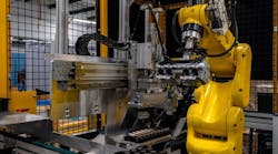
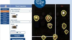
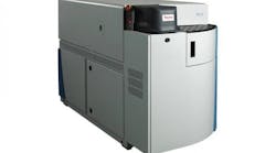
Sonoscan has just shipped the first of its newest next-generation automated bonded wafer inspection systems to a Pacific Rim customer. The new system uses ultra high frequency ultrasound to inspect the critical interface between 2 bonded wafers. If bonding is successful and uniform, and there are no defects, this interface is featureless in acoustic images. But voids, disbonds, cracks and solid particles that can cause failure in subsequent processing steps are sharply defined in the acoustic image. Wafers of 6” and 8” diameters are handled by the new systems, which features a new robotic handler. The system employs a very high-resolution ultrasonic transducer, and images anomalies down to 5 microns in diameter at the interface between the two wafers. The acoustic image made of each bonded wafer pair shows the whole wafer area, including any anomalies. The die pattern can be superimposed onto this image in order to match anomalies with individual die.


